Key Statistics
Key Takeaways
- Market size and growth: the market is estimated at USD 299.6 million in 2026 and is projected to reach USD 544.6 million by 2034, representing a 7.8% CAGR during 2026–2034.
- VGF-grown GaAs is the leading type because low dislocation density and strong crystal uniformity fit high-current-density HBT, LED, laser and other demanding device structures.
- RF applications exceed half of market demand in the underlying market scope, reflecting the continued importance of GaAs power amplifiers, switches and front-end modules in wireless communications.
- Asia Pacific leads, with China identified as the largest individual market and Japan supporting a strong substrate and materials base; Taiwan contributes large GaAs foundry and RF-device demand.
- Larger wafer diameters are a strategic productivity lever: Freiberger lists commercial GaAs wafers up to 200 mm, while 150 mm remains widely used for high-volume RF and optoelectronic device production.
Gallium Arsenide (GaAs) Wafer Market Overview
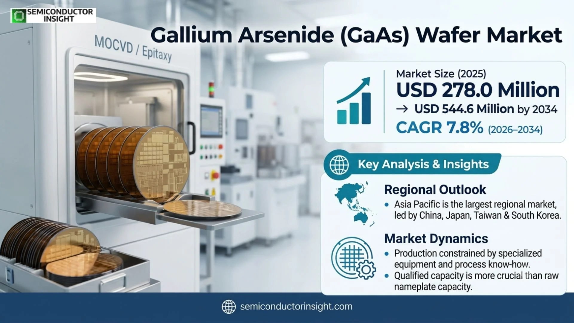
Gallium Arsenide (GaAs) Wafer market was valued at USD 278.0 million in 2025 and is estimated at USD 299.6 million in 2026. The market is projected to reach USD 544.6 million by 2034, representing a CAGR of 7.8% during 2026–2034. Asia Pacific is the largest regional market, led by China, Japan, Taiwan and South Korea across RF devices, optoelectronics, compound-semiconductor foundries and substrate manufacturing.
Base year: 2025 · Estimated year: 2026 · Forecast period: 2026–2034 · Values in USD million unless otherwise stated
Gallium arsenide is a III-V compound semiconductor with a direct bandgap, high electron mobility and strong high-frequency performance. GaAs wafers are used as substrates for RF power amplifiers, switches, HBT and pHEMT devices, LEDs, lasers, VCSELs, detectors and selected high-efficiency photovoltaic cells. The material remains more expensive than silicon, but its electrical and optical properties provide a performance advantage in applications where frequency, efficiency or direct light emission matter more than wafer cost.
Commercial GaAs substrates are produced using crystal-growth techniques such as Vertical Gradient Freeze and Liquid Encapsulated Czochralski. Freiberger states that VGF material is well suited to high-current-density HBT, LED and laser applications, while LEC material serves larger-area devices such as ion-implanted MESFET and pHEMT structures. The supplier lists GaAs wafers from 3-inch through 200 mm, including semi-insulating and semiconducting variants, demonstrating the diversity of electrical specifications used across RF and optoelectronic production.
Demand is anchored by wireless communications but is broadening through VCSEL sensing, automotive radar, datacom lasers and specialty photovoltaics. The transition to 5G and Wi-Fi bands increases RF front-end complexity, while 3D sensing and optical interconnects create additional demand for GaAs-based emitters. The market remains supply-concentrated because high-quality crystal growth, polishing and epi-ready surface preparation require long process know-how and tight control of dislocations, impurities and wafer geometry.
Segment Analysis: By Type
By type, the market is segmented into VGF GaAs, LEC GaAs and other crystal-growth approaches. VGF leads because it can produce low-dislocation-density material with strong uniformity and is used across HBT, pHEMT, LED, laser and solar applications. LEC remains important for selected semi-insulating and semiconducting wafers, particularly where established device processes are qualified around its electrical characteristics and larger crystal-growth history.
| Type | Technical / commercial role | Market position |
|---|---|---|
| VGF GaAs | Vertical Gradient Freeze material with low thermal gradients and strong crystal quality. | Leading segment; widely used for RF, LED, laser and high-current-density devices. |
| LEC GaAs | Liquid Encapsulated Czochralski material grown under encapsulation and pressure. | Established for selected semi-insulating and semiconducting RF/optoelectronic applications. |
| Others | Specialized growth or custom substrate approaches. | Smaller share serving research, legacy and application-specific requirements. |
Segment Analysis: By Application
Applications include RF, LED, VCSEL and photovoltaic devices. RF is the largest segment because GaAs remains highly competitive in handset power amplifiers, switches, wireless infrastructure and satellite communications. LEDs and lasers use the direct bandgap for efficient light emission, while VCSEL demand is linked to sensing and data communications. Photovoltaics remains smaller in unit volume but strategically important in space and other high-efficiency environments where conversion performance matters more than substrate cost.
| Application | Demand characteristics |
|---|---|
| RF | Largest application; power amplifiers, switches, HBT and pHEMT devices for wireless communications. |
| LED | Visible and infrared emitters requiring high-quality semiconducting substrates. |
| VCSEL | 3D sensing, datacom and industrial optical applications using vertical-cavity lasers. |
| Photovoltaic | High-efficiency solar cells for space and specialty energy applications. |
Segment Analysis: By End User
End-user demand is led by telecommunications because mobile devices, base stations, Wi-Fi and satellite systems consume large numbers of GaAs RF components. Consumer electronics contributes through RF front ends and optical sensing. Automotive and industrial applications are growing through radar, LiDAR-related optical emitters and rugged sensing. These sectors value GaAs because its high-frequency or optoelectronic performance can justify the higher substrate cost compared with conventional silicon.
| End User | Demand logic |
|---|---|
| Telecommunications | Largest end user through wireless RF components, satellite links and network infrastructure. |
| Consumer Electronics | Smartphones, wearables and sensing systems support RF and VCSEL demand. |
| Automotive & Industrial | Radar, sensing, optical emitters and specialty high-frequency electronics. |
Segment Analysis: By Wafer Diameter
Wafer diameter directly affects manufacturing economics because larger wafers provide more device area per process cycle but require more difficult crystal-growth and flatness control. Four-inch wafers remain an industry workhorse across mature RF and optoelectronic lines, while six-inch and larger formats are strategic for high-volume production. Freiberger lists 150 mm and 200 mm GaAs products, showing that larger-diameter substrate capability is becoming commercially relevant even though smaller diameters remain deeply installed.
| Wafer Diameter | Commercial role |
|---|---|
| 2-inch & 3-inch | Research, specialty and legacy optoelectronic production. |
| 4-inch | Mature high-volume format with extensive installed fab infrastructure. |
| 6-inch & Above | Higher-throughput growth segment; increasingly important for RF and large-scale production. |
Segment Analysis: By Product Grade
Product grade separates wafers by purity, electrical behavior and intended device class. Semiconductor-grade substrates require tight resistivity, dopant and crystal-defect control for active RF devices. Optoelectronic grades are tailored for LEDs, lasers, VCSELs and detectors, while research and development grades provide lower-volume flexibility for universities and device-development teams. Suppliers monetize value by matching crystal growth, doping and polishing specifications to the final epitaxial and device process rather than selling GaAs as a generic substrate.
| Product Grade | Primary use |
|---|---|
| Semiconductor Grade | RF transistors, switches and integrated high-frequency devices. |
| Optoelectronic Grade | LEDs, lasers, VCSELs, detectors and specialty photovoltaics. |
| Research & Development Grade | Prototype, university and process-development applications. |
Regional Analysis
Asia Pacific is the largest regional market, with China identified as the largest individual market and Japan, Taiwan and South Korea supporting substrate, foundry and device ecosystems. North America remains important through AXT and RF/defense demand, while Europe benefits from Freiberger’s substrate production and strong telecom, automotive and photonics customers. The regional structure reflects both end-market consumption and the location of highly specialized crystal-growth capacity.
GaAs supply is geographically concentrated because wafer production requires specialized crystal-growth equipment and long process experience. Europe and the United States retain important substrate expertise, while Asia contains the largest electronics and RF device manufacturing base. China is expanding compound-semiconductor production and substrate capability, Japan has deep materials expertise, and Taiwan hosts major GaAs foundries. This distributed structure creates cross-border supply chains in which substrates, epitaxy, foundry processing and final modules can occur in different countries.
| Region | Position | Growth outlook | Demand profile | Supplier-selection factor |
|---|---|---|---|---|
| Asia Pacific | Largest | High | RF, foundry, optoelectronics | Quality, local supply and price |
| North America | High-value | Moderate-High | RF, defense, datacom | Performance and domestic supply |
| Europe | Established | Moderate | Substrates, automotive, photonics | Quality and specialty specs |
| South America | Small | Selective | Research / imported devices | Availability |
| Middle East & Africa | Emerging | Selective | Defense / telecom / research | Technical support |
Competitive Landscape
Competition in the Gallium Arsenide (GaAs) Wafer market is shaped by technology performance, customer qualification, application engineering and continuity of supply. Leading companies use product breadth and global support to win large programs, while specialist suppliers can defend attractive niches through deeper technical performance in specific applications. As the market expands, customers increasingly evaluate total system value and lifecycle support rather than relying only on initial component price.
The leading suppliers compete through a combination of proprietary technology, manufacturing scale and customer relationships. In the Gallium Arsenide (GaAs) Wafer market, design wins can remain in place for several product generations because switching suppliers often requires requalification, software changes or manufacturing adjustments. This creates durable revenue positions for vendors that deliver reliable performance and responsive technical support.
Regional suppliers can still gain share where local availability, cost and fast engineering response matter. Their strongest opportunities are generally in standardized or mature applications, while the highest-performance segments remain concentrated among companies with deeper intellectual property, process control and qualification histories. This creates a market structure with both global platform leaders and specialized regional competitors.
Competitive strategy is increasingly moving toward integrated solutions. Customers prefer suppliers that can combine the core product with software, interface components, testing, support or adjacent technologies because integration reduces project risk and development time. Companies able to solve a broader customer problem therefore have more pricing power than vendors competing only on a single specification.
| Competitive tier | Representative companies | Competitive basis |
|---|---|---|
| Global technology leaders | Freiberger Compound Materials, AXT, Inc., Sumitomo Electric Industries, Vital Materials | Scale, broad product portfolios, strong R&D and global customer support. |
| Established specialists | China Crystal Technologies, DOWA Electronics Materials, WIN Semiconductors, Visual Photonics Epitaxy | Application-specific engineering and strong qualification in selected segments. |
| Regional / emerging suppliers | IQE, Advanced Wireless Semiconductor Company, MTI Corporation, PAM-XIAMEN | Local service, competitive pricing and focused customer relationships. |
Key Participants
The profiled competitive set includes Freiberger Compound Materials, AXT, Inc., Sumitomo Electric Industries, Vital Materials, China Crystal Technologies, DOWA Electronics Materials, WIN Semiconductors, Visual Photonics Epitaxy, IQE, Advanced Wireless Semiconductor Company, MTI Corporation, PAM-XIAMEN. Supplier position depends on engineering performance, customer qualification, manufacturing continuity and the ability to support design changes over long product cycles. Larger vendors benefit from broad portfolios and application teams, while specialists can retain strong positions in narrow, technically demanding subsegments where historical qualification and process know-how create meaningful switching costs.
Production Capacity Analysis
Production capacity for Gallium Arsenide (GaAs) Wafer is constrained by the combination of specialized equipment, qualified materials, process know-how and customer-specific validation. Nominal factory output can overstate commercial supply because a new line or material source must often demonstrate consistent performance before it can serve high-value customers. This makes qualified capacity more important than raw nameplate capacity.
Regional manufacturing and service capacity influence lead time and resilience. Customers increasingly prefer suppliers that can support major production clusters from more than one site, reducing exposure to logistics disruption and single-factory events. At the same time, duplicating specialized processes can be difficult because equipment recipes, trained engineers and quality systems must be transferred without changing product performance.
The strongest capacity investments are aligned with structural demand drivers rather than short-term cycles. Suppliers expanding around AI, advanced semiconductor manufacturing, automotive electronics or industrial automation seek to secure positions before customer volumes scale. Effective capacity therefore includes engineering resources, test capability and local technical support in addition to physical manufacturing equipment.
| Capacity factor | Market implication |
|---|---|
| Specialized manufacturing | Determines qualified output and technical performance. |
| Critical materials / components | Can constrain supply despite available factory floor space. |
| Qualification and test | Controls how quickly new capacity becomes usable by customers. |
| Regional support | Improves lead time, resilience and customer retention. |
Market Dynamics
The Gallium Arsenide (GaAs) Wafer market is driven by higher system performance, automation, digitalization and expanding use in high-value applications. Growth is moderated by development cost, qualification requirements and supply-chain concentration. The strongest opportunities occur where new architectures or applications create a clear performance advantage and where suppliers can reduce integration complexity for customers.
MARKET DRIVERS
| Driver | Relative impact | Commercial mechanism |
|---|---|---|
| Structural end-market growth | High | Expanding deployments increase unit demand and installed-base requirements. |
| Technology upgrade cycle | High | Higher performance raises value per product and accelerates replacement. |
| Customer integration needs | Medium-High | Validated solutions reduce engineering time and project risk. |
| Regional capacity expansion | Medium | New manufacturing clusters create local supplier demand. |
Structural end-market expansion
Growth in the Gallium Arsenide (GaAs) Wafer market is supported by rising deployment across its principal applications. Customers are investing because the technology improves performance, efficiency, automation or product capability in ways that are difficult to replicate with older approaches. This expands both new-system demand and the installed base that later requires replacement, upgrades or related services.
Higher technical requirements increase value per system
New product generations demand tighter performance, greater integration and better reliability. These requirements can increase selling prices even when unit volumes grow more slowly, because customers are willing to pay for solutions that protect yield, uptime or user experience. Suppliers with stronger engineering capability therefore benefit disproportionately from technology transitions.
Regional investment broadens customer access
Manufacturing and infrastructure investment in North America, Europe and Asia is creating additional customer clusters outside traditional centers. Local engineering support and shorter supply chains help suppliers qualify products earlier in new projects, creating an opportunity to win design positions before production reaches full scale.
MARKET RESTRAINTS
| Restraint | Relative impact | Commercial mechanism |
|---|---|---|
| Development and qualification cost | High | Raises barriers to entry and lengthens customer adoption. |
| Supply-chain concentration | Medium-High | Critical components or materials can limit output. |
| Price pressure | Medium | Customers seek lower total system cost as volumes increase. |
| Technology substitution | Medium | Alternative architectures can replace incumbent solutions in selected uses. |
Qualification slows supplier switching
Customers in technical markets cannot change suppliers based only on purchase price. New products must demonstrate performance, reliability and compatibility in the actual application, which can require months of engineering work. This limits the pace at which new entrants gain share and can delay commercialization of technically promising products.
Specialized inputs can constrain supply
Advanced products depend on a limited number of qualified materials, components or manufacturing tools. Shortages or long lead times at one upstream stage can restrict finished-product output even when downstream assembly capacity is available. Suppliers therefore carry strategic inventory or qualify alternate sources, but those actions increase cost.
Customer cost pressure remains persistent
As a technology becomes more widely adopted, customers expect lower unit costs and may redesign systems to use standardized components. Suppliers must offset this pressure through better performance, lower manufacturing cost and additional software or service value. Vendors that cannot maintain differentiation can face margin erosion even in a growing market.
MARKET OPPORTUNITIES
Larger-diameter GaAs wafers
Moving from 100 mm to 150 mm and eventually 200 mm substrates increases device area processed per wafer and can lower cost for high-volume RF and optoelectronic products. The opportunity favors crystal growers that can maintain low defect density, flatness and electrical uniformity as diameter increases. Larger wafers also allow existing silicon-style automation concepts to be used more effectively.
VCSEL and optical interconnect growth
VCSELs are used in sensing and data communications, both of which benefit from GaAs’s direct bandgap and mature epitaxial ecosystem. Growth in optical links for AI data centers and continued 3D sensing can expand demand beyond traditional handset RF. Suppliers positioned with low-defect semiconducting wafers can capture higher-value optoelectronic programs.
Automotive radar and sensing
Advanced driver-assistance systems increase the number of radar and sensing functions per vehicle. While some RF markets are shifting toward alternative materials, GaAs remains relevant in selected high-frequency and optical applications. Automotive qualification creates long program lifetimes, giving substrate suppliers an opportunity to build durable revenue once a material specification is approved.
Specialty and space photovoltaics
GaAs solar cells deliver very high efficiency and radiation resistance, making them attractive for satellites and specialty aerospace systems where cost per watt is less important than performance. Growth in satellite constellations and space infrastructure can sustain premium wafer demand even though volumes remain far below RF and consumer electronics.
Supply Chain Analysis
Specialized materials and components
Core product manufacturing
Qualification and system integration
End-user deployment, service and replacement
The upstream supply chain provides the specialized materials, semiconductor devices, mechanical components or substrates that determine baseline product performance. Qualified inputs are important because changes in composition or manufacturing source can alter reliability, electrical behavior or process compatibility. Suppliers therefore maintain close technical relationships with upstream partners and often approve alternate sources before a disruption occurs.
Manufacturing converts these inputs into finished products using process-specific equipment, inspection and test. Quality systems are central because customers expect lot-to-lot consistency and traceability, particularly in semiconductor, automotive and industrial applications. High-value suppliers differentiate through process control rather than simple assembly scale, and they invest heavily in metrology or validation to protect yield.
Downstream value is created when the product is integrated into the customer system and validated under real operating conditions. Application engineers support installation, software, calibration or process optimization, while service teams maintain the installed base. This lifecycle relationship creates recurring revenue through replacement, updates, refurbishment or expansion and makes customer support an important part of the market structure.
Recent Developments
2026 – Freiberger lists commercial GaAs wafers up to 200 mm
Freiberger’s current product specifications include 150 mm and 200 mm GaAs wafers, with semi-insulating and semiconducting options for HBT, pHEMT, solar and optoelectronic applications, highlighting the industry’s movement toward larger substrates. Source
2026 – VGF remains central to low-defect GaAs crystal growth
Freiberger describes VGF crystal growth with low axial thermal gradients and positions the method for high-current-density HBT, LED and laser devices, underscoring the importance of crystal-quality control in commercial wafer production. Source
2026 – 6-inch semi-insulating GaAs supports state-of-the-art wireless devices
Freiberger identifies 6-inch semi-insulating GaAs as a production substrate for HBT, pHEMT and BiFET wireless devices, linking larger wafer formats directly to high-volume RF front-end manufacturing. Source
REPORT SCOPE & SEGMENTATION
| Base Year | 2025 |
| Estimated Year | 2026 |
| Forecast Year | 2034 |
| 2025 Market Size | USD 278.0 million |
| 2026 Market Size | USD 299.6 million |
| 2034 Market Size | USD 544.6 million |
| CAGR | 7.8% during 2026–2034 |
| Largest Market / Leading Geography | Asia Pacific |
| By Type | VGF GaAs; LEC GaAs; Others |
| By Application | RF; LED; VCSEL; Photovoltaic |
| By End User | Telecommunications; Consumer Electronics; Automotive & Industrial |
| By Wafer Diameter | 2-inch & 3-inch; 4-inch; 6-inch & Above |
| By Product Grade | Semiconductor Grade; Optoelectronic Grade; Research & Development Grade |
Frequently Asked Questions
What is the size of the GaAs wafer market?
The market is estimated at USD 299.6 million in 2026 and is projected to reach USD 544.6 million by 2034, representing a 7.8% CAGR during 2026–2034. The 2025 market size is USD 278.0 million.
Which GaAs wafer type leads the market?
VGF-grown GaAs leads because its low-defect crystal quality and uniformity support high-current-density RF and optoelectronic devices.
Which application is largest?
RF is the largest application, supported by GaAs power amplifiers, switches and other front-end components used in smartphones, wireless infrastructure and satellite systems.
Which wafer diameter is most important?
Four-inch wafers remain widely installed, while six-inch and larger formats are the strategic growth area because they can improve throughput and economics in high-volume production.
Which region leads the market?
Asia Pacific leads because China, Taiwan, Japan and South Korea combine the largest RF-device, foundry and electronics manufacturing ecosystems.
What are the main restraints?
High substrate cost, crystal-growth complexity, raw-material concentration and competition from GaN or SiC in selected applications are the main restraints.
Research Sources & Evidence Base

Get Sample Report PDF for Exclusive Insights
Report Sample Includes
- Table of Contents
- List of Tables & Figures
- Charts, Research Methodology, and more...
 Download Sample Report PDF